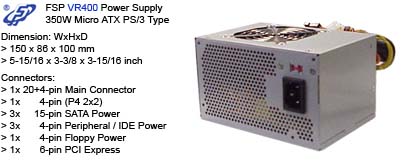
Micro ATX Switching Power
Supply
FSP VR400 PS3 (PS/3)
Type
PS-PS3-FSP350-VR400
Down Load:
Dimension: WxHxD
- 150 x 86 x 100 mm
- 5.91 x 3.39 x 3.94 inch
- 5-15/16 x 3-3/8 x 3-15/16 inch
Connectors:
- 1x 20+4-pin Main Connector
- 1x 4-pin (P4 2x2)
- 3x 15-pin SATA Power
- 3x 4-pin Peripheral / IDE Power
- 1x 4-pin Floppy Power
- 1x 6-pin PCI Express
Input
Electrical Specifications
- AC Input
|
Parameter |
Min. |
Nom.(1) |
Max. |
Unit |
|
Vin (115VAC) |
103.5 |
115 |
132 |
VAC rms |
|
Vin Frequency |
57 |
-- |
63 |
HZ |
|
Vin (230VAC) |
207 |
230 |
264 |
VAC rms |
|
Vin Frequency |
47 |
-- |
53 |
HZ |
|
*
Nominal voltages
for test purposes are considered to be within
±1.0V
of nominal. |
- Inrush
Current
Maximum inrush
current from power-on (with power on at any point on the AC sine) and
including, but not limited to, three line cycles, shall be limited to a
level below the surge rating of the input line cord, AC switch if
present, bridge rectifier, fuse, and EMI filter components. Repetitive
ON/OFF cycling of the AC input voltage should not damage the power
supply or cause the input fuse to blow.
- Input
Line Current
|
AC Input |
Input Line Current |
|
115V |
< 7.5Amps - rms |
|
230V |
< 4.5Amps - rms |
Efficiency
- General
Under the
load conditions defined in Table 1 and Table 2. The loading
condition for testing efficiency shown in Table 1 represents a fully
loaded system. a ~ 50-60% (typical) loaded system, and a ~ 20-30%
(light) loaded system.
- Loading Table for
Efficiency Measurements
|
350W (loading shown in Amps) |
|
Loading |
+12V1 |
+12V2 |
+5V |
+3.3V |
-12V |
+5Vsb |
|
Full |
9.5 |
11.2 |
9.2 |
12.9 |
0.3 |
2.1 |
|
Typical |
4.7 |
5.6 |
4.6 |
6.4 |
0.1 |
1.1 |
|
Light |
1.9 |
2.2 |
1.8 |
2.6 |
0.1 |
0.4 |
- Minimum Efficiency Vs Load
|
Loading |
Voltage |
Full Load |
Typical Load |
Light Load |
|
Required Minimum Efficiency |
115V |
70% |
75% |
70% |
|
Required Minimum Efficiency |
230V |
75% |
75% |
70% |
Output Electrical Requirements
- Output Voltage and Current Rating
|
Output Voltage |
Minimum Load |
Normal Load |
Maximum Load |
Peak Load |
Load Reg. |
Line Reg. |
Ripple Noise |
|
+3.3V |
0.1A |
10.5A |
21A |
--- |
± 5% |
± 1% |
70mV P-P |
|
+5V |
0.2A |
7.5A |
15A |
--- |
± 5% |
± 1% |
70mV P-P |
|
+12V1 |
0.1A |
8A |
16A |
20A |
± 5% |
± 1% |
140mV P-P |
|
+12V2 |
0.5A |
7A |
14A |
18A |
± 5% |
± 1% |
140mV P-P |
|
-12V |
0.0A |
0.15A |
0.3A |
--- |
± 10% |
± 1% |
140mV P-P |
|
+5Vsb |
0.0A |
1.25A |
2.5A |
3.5A |
± 5% |
± 1% |
70mV P-P |
( 1 ).+3.3V & +5V total
output not exceed 103W.
( 2 ).Maximum combined current for the 12V outputs shall be 22A.
( 3 ).Total output for this subject power supply is 350 watts, peak
load 400 watts.
( 4 ).The maximum continuous power rating of supply is 350W at 40°C.
( 5 ).+12V1 Peak current is 20A(less than 10m Sec.), minimum
voltage during peak is >10.8Vdc.
( 6 ). +12V2 Peak current is 18A(less than 10m Sec.), minimum
voltage during peak is >10.8Vdc.
( 7 ). 5Vsb peak current is 3.5A(less then 500mSec.), minimum
voltage during peak is > 4.5Vdc.
( 8 ).Voltages and ripple are
measured at the load side of mating connectors with a 0.1 uF
monolithic ceramic capacitor
paralleled by a 10 uF electrolytic capacitor across the measuring
terminals. |
- Load Capacity Specifications
The cross regulation defined as follows, the voltage regulation
limits DC include DC Output ripple & noise.
|
Load |
+3.3V |
+5V |
+12V1 |
+12V2 |
-12V |
+5VSB |
|
Conditin_1 |
x |
x |
x |
x |
x |
2.0 |
|
Conditin_2 |
2 |
0.2 |
0.1 |
0.5 |
0 |
2.5 |
|
Conditin_3 |
0.1 |
2 |
0.5 |
0.5 |
0.3 |
0 |
|
Conditin_4 |
4 |
4.5 |
16 |
6 |
0.3 |
1 |
|
Conditin_5 |
1 |
15 |
3 |
3 |
0.1 |
0 |
|
Conditin_6 |
10 |
3 |
3 |
3 |
0 |
0.1 |
|
Conditin_7 |
21 |
6.7 |
11 |
1 |
0.3 |
0.1 |
|
Conditin_8 |
8.48 |
15 |
1 |
14 |
0.1 |
0.1 |
|
Conditin_9 |
12 |
6.5 |
9.5 |
10 |
0.3 |
2 |
-
HOLD-UP TIME (@ Typical Load of Table 1.)
115V / 60Hz : 17 m Sec. Minimum.
230V / 50Hz : 17 m Sec. Minimum.
The output voltage will remain within specification, in the event
that the input power is removed or interrupted, for the duration of
one cycle of the input frequency. The interruption may occur at any
point in the AC voltage cycle. The power good signal shall remain
high during this test.
-
Output Rise Time
(10% TO 95% OF FINAL OUTPUT VALUE, @FULL LOAD of Table 1.)
115V-rms or 230V-rms + 3.3Vdc : 20ms Maximum
+ 5Vdc : 20ms Maximum
+ 12Vdc : 20ms Maximum
+ 5Vsb : 20ms Maximum
- 12Vdc : 20ms Maximum
- Over Voltage Protection
|
Voltage Source |
Protection Point |
|
+3.3V |
3.76V~4.8V |
|
+5V |
5.6V~7.0V |
|
+12V |
13.0V~16.5V |
-
Short Circuit Protection
Output short circuit is defined to be a short circuit load of less
than 0.1 ohm. In the event of an output short circuit condition on
+3.3V, +5V, +12V,-12V output, the power supply will shutdown and
latch off without damage to the power supply. The power supply shall
return to normal operation after the short circuit has been removed
and the power switch has been turned off for no more than 2 seconds.
- Power Signal
Power Good @115/230V, Full Load of
Table 1. 100~500m Sec.
Power Fail @115/230V, Full Load of Table 1. 1m Sec. Minimum

T1: Power-on time shall be less than 500 ms (T1 < 500 ms).
T2: Rise time : 0.1 ms to 20 ms (0.1 ms ≤ T2
≤ 20 ms).
T3: Power-ok delay time: 100 ms < T3 < 500 ms
T4: Power-ok rise time: T4 ≦ 1 ms
T5 + T6: AC loss to PWR_OK hold-up time :T5 + T6 ≥
17 ms
Environmental Requirements
The power supply will be compliant with each item in
this specification for the following Environmental Conditions
-
Temperature Range
Operating +10 to +40 deg. C
Storage -20 to +80 deg. C
The maximum continuous power rating of supply is 350W at 40℃.
-
Humidity
Operating 5 –95% RH, Non-condensing
Storage 5 –95% RH, Non-condensing
-
Vibration
The subject power supply will withstand the following imposed
conditions without experiencing non-recoverable failure or deviation
from specified output characteristics. Vibration Operating – Sine
wave excited, 0.25 G maximum acceleration, 10-250 Hz swept at one
octave / min. Fifteen minute dwell at all resonant points, where
resonance is defined as those exciting frequencies at which the
device under test experiences excursions two times large than
non-resonant excursions. Plane of vibration to be along three
mutually perpendicular axes.
-
Ground Leakage Current
The power supply ground leakage current shall be less than 3.5
mA.
-
Reliability
The power supply reliability, when calculated by MIL-HDBK-217;latest
revision, are exceed 100,000 hours with all output at typical load
and an ambient temperature of 25℃.
-
Dielectric Strength
Primary to Frame Ground : 1800 Vac for 1 sec.
Primary to Secondary : 1800 Vac for 1 sec
-
Insulation Resistance
Primary to Frame Ground : 20 Meg. ohms Minimum
Primary to Secondary : 20 Meg. ohms Minimum
Labeling
Label marking will be permanent, legible and complied with all
agency requirements.
-
Model Number Label
Labels will be affixed to the sides of the power supply showing the
following:
- Manufacturer’s name and logo.
- Model no., serial no., revision level, location of manufacturer.
- The total power output and the maximum load for each output.
- AC input rating.
Mechanical Specifications
The mechanical drawing of the subject power supply, which indicate
the form factor, location of the mounting holes, location, the length of
the connectors, and other physical specifications of the subject power
supply. Please refer to the attachment drawing. |